The Triforce arcade platform is essentially a GameCube sandwiched between some other custom SEGA and Namco hardware, and the ham and cheese of that sandwich is the main board: A nearly-stock GameCube motherboard that looks identical to the DOL-001 variant.
Of course, it's not 100% identical. One of the most notable differences is the bootrom. If you boot a Triforce with the media board disconnected, you'll get an error:
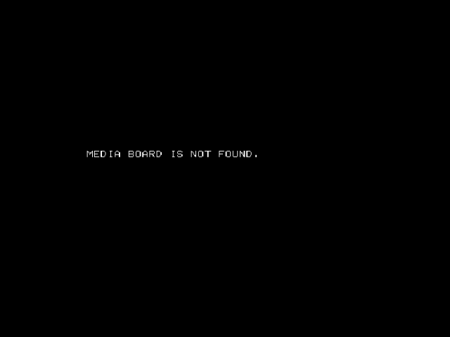
This error is from the Triforce bootrom.
In a proper Triforce, what happens next is that the bootrom issues a slew of DI commands, among probably some other things, loading and executing a payload from the media board known as SegaBoot. SegaBoot is what actually displays the Triforce logo at boot.
Today I want to focus on a more boring thing: The very first instructions that get executed, sometimes known as 'BS1' or Bootstrap Stage 1.
For the most part, the Triforce BS1 is not materially different from a retail GameCube. It looks like it may be even more similar to the GDEV bootrom, based on induction, but I don't have access to a GDEV to confirm this. Nevertheless, I thought this would be a useful learning experience, so I finished it anyways.
Prior Art
Almost everything I'm digging into today is prior art. There's a lot of good documentation floating around for the GameCube boot process, and in particular, the following documents helped me along a fair bit:
YAGCD, or “Yet Another GameCube Documentation”
https://www.gc-forever.com/yagcd/The gcforever wiki page on the bootrom.
https://www.gc-forever.com/wiki/index.php?title=BootromData sheets and PowerPC documentation, such as “PowerPC® Microprocessor Family: The Programming Environments Manual”.
Bootstrap Stage 1
The GameCube memory map looks like this. Right?
| Address | Description |
|---|---|
0x80000000 | System Memory (write-back) |
0xC0000000 | System Memory (write-through) |
0xC8000000 | Embedded Frame Buffer (EFB) |
0xCC000000 | Hardware Registers |
0xFFF00000 | Bootrom |
Well, kind of. That's what it looks like to most software. But the bootrom is different, because the bootrom runs before Gekko's Block Address Translation is configured. (It's the bootrom that configures it!)
The actual memory map starts out looking more like this:
| Address | Description |
|---|---|
| 0x00000000 | System Memory |
| 0x08000000 | Embedded Frame Buffer (EFB) |
| 0x0C000000 | Hardware Registers |
| 0xFFF00000 | Bootrom |
These are the physical addresses that are wired in hardware, and it's what things look like where we begin.
Which is a good segue. We begin executing at 0xFFF00100, which is 0x100 bytes into the bootrom. (The gcforever wiki has more information on why this address.)
What even is the bootrom? It's actually a tiny serial device that includes, as well, some SRAM and an RTC. It lives on the EXI bus, a bus very similar to (and roughly compatible with) SPI. Another important detail is the scrambler. When the scrambler is on, each byte read from the bootrom will be descrambled. Note that the scrambler is not enabled when reading all of the bytes; some data in the bootrom is not encrypted, including the first 256 bytes, and some fonts. Also, the scrambler is 'dumb'; it is not aware of what offset you're reading. So if you were to read a byte out of order, the results would be different.
So that's where we start. So far, everything is, as far as anyone knows, essentially identical between a Triforce mainboard and a GameCube motherboard.
First Steps
0fff00100  3c800011   lis     r4, 0x11
0fff00104  38840c64   addi    r4, r4, 0xc64
0fff00108  7c90fba6   mtspr   0x3f0, r4  // Set HID0 to 0x00110c64
0fff0010c  3c800000   lis     r4, 0x0
0fff00110  38842000   addi    r4, r4, 0x2000
0fff00114  7c800124   mtmsr   r4  // Set machine state register to 0x2000
Same as retail GameCube. This segment sets some registers that control hardware features like branch prediction, caches, exception handling, etc. Most importantly, the instruction cache is enabled. This is important because once instructions are cached, they are not fetched again until they get evicted from the cache or the cache is invalidated. This enables us to use non-linear control flow while keeping the EXI accesses linear so that the scrambler stays in sync.
ARAM Initialization
0fff00118  3c800c00   lis     r4, 0xc00
0fff0011c  38845012   addi    r4, r4, 0x5012
0fff00120  38a00003   li      r5, 0x3
0fff00124  b0a40000   sth     r5, 0(r4)  // Set 0x5012 register value to 0x03.
0fff00128  38a0009c   li      r5, 0x9c
0fff0012c  b0a40008   sth     r5, 8(r4)  // Set 0x501A register (ARAM refresh) to 0x9c (156 MHz)
Differs from retail GameCube. This code is similar to the retail GameCube, but it sets the 0x5012 register to 0x03, whereas retail GameCube sets it to 0x43. The significance of this bit is not known. Dolphin calls this register AR_INFO, whereas YAGCD calls it AR_SIZE. It has been noted on the gcforever bootrom wiki page that the "last two bits are set only when ARAM expansion is present" but it's unclear if they're referring to least or most significant bits and what is meant by "ARAM expansion" (i.e. how much additional memory? Did the GameCube ship with this? Rumors from 2001 suggest it did not.)
Flipper Memory Interface Initialization (?)
0fff00130  3c600c00   lis     r3, 0xc00
0fff00134  60634000   ori     r3, r3, 0x4000
0fff00138  38800040   li      r4, 0x40
0fff0013c  b0830026   sth     r4, 38(r3)  // Set 0x4026 register value to 0x40.
0fff00140  60000000   nop
0fff00144  60000000   nop
Same as retail GameCube. Supposedly, this has something to do with initializing the Flipper memory interface, although it's not known exactly what the register actually does.
Enable CPU caches
0fff00148  7c70faa6   mfspr   r3, 0x3f0
0fff0014c  6064c000   ori     r4, r3, 0xc000
0fff00150  7c90fba6   mtspr   0x3f0, r4  // Enable data and instruction cache.
0fff00154  60000000   nop
0fff00158  60000000   nop
0fff0015c  60000000   nop
0fff00160  4c00012c   isync
Same as retail GameCube. Sets Instruction Cache Enable and Data Cache Enable flags.
Clear BAT/Segment registers
0fff00164  38800000   li      r4, 0x0  // Zero out DBAT/IBAT registers.
0fff00168  7c9883a6   mtdbatu DBAT0U, r4
0fff0016c  7c9a83a6   mtdbatu DBAT1U, r4
0fff00170  7c9c83a6   mtdbatu DBAT2U, r4
0fff00174  7c9e83a6   mtdbatu DBAT3U, r4
0fff00178  7c9083a6   mtibatu IBAT0U, r4
0fff0017c  7c9283a6   mtibatu IBAT1U, r4
0fff00180  7c9483a6   mtibatu IBAT2U, r4
0fff00184  7c9683a6   mtibatu IBAT3U, r4
0fff00188  4c00012c   isync
0fff0018c  3c808000   lis     r4, 0x8000  // Set all segment registers to 0x80000000.
0fff00190  38840000   addi    r4, r4, 0x0
0fff00194  7c8001a4   mtsr    0x0, r4
0fff00198  7c8101a4   mtsr    0x1, r4
0fff0019c  7c8201a4   mtsr    0x2, r4
0fff001a0  7c8301a4   mtsr    0x3, r4
0fff001a4  7c8401a4   mtsr    0x4, r4
0fff001a8  7c8501a4   mtsr    0x5, r4
0fff001ac  7c8601a4   mtsr    0x6, r4
0fff001b0  7c8701a4   mtsr    0x7, r4
0fff001b4  7c8801a4   mtsr    0x8, r4
0fff001b8  7c8901a4   mtsr    0x9, r4
0fff001bc  7c8a01a4   mtsr    0xa, r4
0fff001c0  7c8b01a4   mtsr    0xb, r4
0fff001c4  7c8c01a4   mtsr    0xc, r4
0fff001c8  7c8d01a4   mtsr    0xd, r4
0fff001cc  7c8e01a4   mtsr    0xe, r4
0fff001d0  7c8f01a4   mtsr    0xf, r4
Same as retail GameCube. It is necessary, prior to setting up any memory mapping, to clear the BAT and segment registers, as they are not initialized on power-on.
Set up Block Address Translation
0fff001d4  3c800000   lis     r4, 0x0
0fff001d8  38840002   addi    r4, r4, 0x2
0fff001dc  3c608000   lis     r3, 0x8000
0fff001e0  38631fff   addi    r3, r3, 0x1fff
0fff001e4  7c9983a6   mtdbatl DBAT0L, r4
0fff001e8  7c7883a6   mtdbatu DBAT0U, r3
0fff001ec  4c00012c   isync
0fff001f0  7c9183a6   mtibatl IBAT0L, r4
0fff001f4  7c7083a6   mtibatu IBAT0U, r3
0fff001f8  4c00012c   isync
0fff001fc  3c800000   lis     r4, 0x0
0fff00200  3884002a   addi    r4, r4, 0x2a
0fff00204  3c60c000   lis     r3, 0xc000
0fff00208  38631fff   addi    r3, r3, 0x1fff
0fff0020c  7c9b83a6   mtdbatl DBAT1L, r4
0fff00210  7c7a83a6   mtdbatu DBAT1U, r3
0fff00214  4c00012c   isync
0fff00218  3c80fff0   lis     r4, 0xfff0
0fff0021c  38840001   addi    r4, r4, 0x1
0fff00220  3c60fff0   lis     r3, 0xfff0
0fff00224  3863001f   addi    r3, r3, 0x1f
0fff00228  7c9f83a6   mtdbatl DBAT3L, r4
0fff0022c  7c7e83a6   mtdbatu DBAT3U, r3
0fff00230  4c00012c   isync
0fff00234  7c9783a6   mtibatl IBAT3L, r4
0fff00238  7c7683a6   mtibatu IBAT3U, r3
0fff0023c  4c00012c   isync
Same as retail GameCube. This sets up the block address translation registers. Out of four each, only 2 DBAT and 3 IBAT registers are used.
They are set up like this:
DBAT0L, DBAT0U = 0x0000_0002, 0x8000_1fff
DBAT1L, DBAT1U = 0x0000_002a, 0xc000_1fff
DBAT3L, DBAT3U = 0xfff0_0001, 0xfff0_001f

IBAT0L, IBAT0U = 0x0000_0002, 0x8000_1fff
IBAT3L, IBAT3U = 0xfff0_0001, 0xfff0_001f
Here's what's in a BAT register, mapped out from Section 2.3.3 of PowerPC Microprocessor Family: The Programming Environments:
BATL: 0bAAAA_AAAA_AAAA_AAA#_####_####_#WIM_G#PP
- A: Block Real Page Number. High bits of the physical address.
- #: Reserved.
- W: Write-through
- I: Cache-inhibiting
- M: Memory coherence
- G: Guarded
- P: Protection bits. Inaccessible, read-only or read-write.

BATU: 0bIIII_IIII_IIII_III#_###L_LLLL_LLLL_LLSU
- I: Block Effective Page Index. High bits of the logical/effective address.
- #: Reserved.
- L: Block length. BS1 only uses 256 MiB blocks, which is all-bits-set.
- S: Supervisor mode. Defines if block is visible to instructions executed at supervisor privilege.
- U: User mode. Defines if the block is visible to instructions executed at user mode privilege.
When applied to the BAT values above, we can see that it gives us the familiar GameCube memory map, including the memory-mapped registers which are accessed through the write-through BAT.
Enable Address Translation
0fff00240  7c8000a6   mfmsr   r4
0fff00244  60840030   ori     r4, r4, 0x30
0fff00248  7c800124   mtmsr   r4
0fff0024c  4c00012c   isync
Same as retail GameCube. After clearing the segment registers and setting up the BAT, it's now time to actually enable address translation.
Unknown Processor Configuration
0fff00250  3c60cc00   lis     r3, 0xcc00
0fff00254  60633000   ori     r3, r3, 0x3000
0fff00258  3c800245   lis     r4, 0x245
0fff0025c  6084248a   ori     r4, r4, 0x248a
0fff00260  90830030   stw     r4, 48(r3)
Same as retail GameCube. Note that we're now accessing registers through the logical addresses set forth by the BAT registers.
Memory Initialization
0fff00264  80830024   lwz     r4, 36(r3)  // Read reset register
0fff00268  60840001   ori     r4, r4, 0x1  // |= 1
0fff0026c  548407f8   rlwinm  r4, r4, 0x0, 0x1f, 0x1c  // & ~6
0fff00270  90830024   stw     r4, 36(r3)  // Write to reset register

// Busy-wait for 5000 clocks (~10 us)
0fff00274  7cac42e6   mftb    r5, 0x10c
0fff00278  7ccc42e6   mftb    r6, 0x10c
0fff0027c  7ce53050   subf    r7, r5, r6
0fff00280  28071388   cmplwi  r7, 5000
0fff00284  4180fff4   blt     0xfff00278

0fff00288  60840003   ori     r4, r4, 0x3  // |= 3
0fff0028c  90830024   stw     r4, 36(r3)  // Write to reset register

// Busy-wait for 1024 clocks (~2 us)
0fff00290  7cac42e6   mftb    r5, 0x10c
0fff00294  7ccc42e6   mftb    r6, 0x10c
0fff00298  7ce53050   subf    r7, r5, r6
0fff0029c  28070400   cmplwi  r7, 0x400
0fff002a0  4180fff4   blt     0xfff00294

0fff002a4  3c80c000   lis     r4, 0xc000
0fff002a8  3ca0ffff   lis     r5, 0xffff
0fff002ac  3cc00000   lis     r6, 0x0

// Set some bytes in main memory.
0fff002b0  90a40000   stw     r5, 0(r4)  // MEMORY[0c0000000] = 0xffff
0fff002b4  90c40010   stw     r6, 16(r4)  // MEMORY[0c0000010] = 0x0
0fff002b8  90c40020   stw     r6, 32(r4)  // MEMORY[0c0000020] = 0x0
0fff002bc  90a40030   stw     r5, 48(r4)  // MEMORY[0c0000030] = 0xffff

// If any of the bytes don't match, start over and try again.
0fff002c0  80e40000   lwz     r7, 0(r4)
0fff002c4  7c053800   cmpw    r5, r7  // if (MEMORY[0c0000000] != 0xffff)
0fff002c8  4082ff9c   bne     0xfff00264  // goto 0xfff00264

0fff002cc  80e40010   lwz     r7, 16(r4)
0fff002d0  7c063800   cmpw    r6, r7  // if (MEMORY[0c0000010] != 0x0)
0fff002d4  4082ff90   bne     0xfff00264  // goto 0xfff00264

0fff002d8  80e40020   lwz     r7, 32(r4)
0fff002dc  7c063800   cmpw    r6, r7  // if (MEMORY[0c0000020] != 0x0)
0fff002e0  4082ff84   bne     0xfff00264  // goto 0xfff00264

0fff002e4  80e40030   lwz     r7, 48(r4)
0fff002e8  7c053800   cmpw    r5, r7  // if (MEMORY[0c0000030] != 0xffff)
0fff002ec  4082ff78   bne     0xfff00264  // goto 0xfff00264

0fff002f0  60000000   nop
0fff002f4  60000000   nop
0fff002f8  60000000   nop
0fff002fc  60000000   nop
Differs from retail GameCube. After the first write to reset, the real GameCube only waits 4388 clocks, whereas Triforce waits 5000 clocks. Then, Triforce waits 1024 clocks after the second write to reset.
After doing the magic register writes needed to initialize the memory, a small test is done to see if it appears to be coherent. If not, the process is restarted again. This is not present on retail GameCube.
The retail GameCube BS1 also performs a memory test here; that is also not present.
Copy BS2 to Main Memory
Enable 32MHz EXI transfers
// Enable 32MHz EXI clock
0fff00300  3dc0cc00   lis     r14, 0xcc00
0fff00304  61ce6400   ori     r14, r14, 0x6400
0fff00308  38800000   li      r4, 0x0
0fff0030c  908e003c   stw     r4, 60(r14)
Same as retail GameCube.
Set up GPRs for BS2 transfer
0fff00310  3c40cc00   lis     r2, 0xcc00
0fff00314  60426800   ori     r2, r2, 0x6800  // Load EXI register block base into r2
0fff00318  3cc00000   lis     r6, 0x0
0fff0031c  // Load EXI flags into r6: 0b0101010000
0fff0031c  // EXTINTMASK = 0   - disable
0fff0031c  // EXTINT     = 0   - do nothing
0fff0031c  // TCINTMASK  = 0   - disable
0fff0031c  // TCINT      = 0   - do nothing
0fff0031c  // CLK        = 101 - 32 MHz
0fff0031c  // CS         = 010 - select device 1
0fff0031c  // EXTINTMASK = 0   - disable
0fff0031c  // EXTINT     = 0   - disable
0fff0031c  // ROMDIS     = 0   - do nothing
0fff0031c  60c60150   ori     r6, r6, 0x150
0fff00320  3ce00000   lis     r7, 0x0
0fff00324  // Load EXI control register flags into r7: 0x35 = 0b110101
0fff00324  //  TSTART = 1  - start transfer
0fff00324  //  DMA    = 0  - immediate mode
0fff00324  //  RW     = 01 - write
0fff00324  //  TLEN   = 11 - 4 bytes
0fff00324  60e70035   ori     r7, r7, 0x35
0fff00328  39000001   li      r8, 0x1  // r8 = 1; Used as a bitmask.
0fff0032c  3d200000   lis     r9, 0x0
0fff00330  // Load EXI control registr flags into r9: 0x3 = 0b000011
0fff00330  //  TSTART = 1  - start transfr
0fff00330  //  DMA    = 1  - DMA
0fff00330  //  RW     = 00 - read
0fff00330  //  TLEN   = unused
0fff00330  61290003   ori     r9, r9, 0x3
0fff00334  39400000   li      r10, 0x0  // r10 = 0
0fff00338  3d600000   lis     r11, 0x0
0fff0033c  616b0400   ori     r11, r11, 0x400  // r11 = 0x400
0fff00340  3d800001   lis     r12, 0x1
0fff00344  618c0000   ori     r12, r12, 0x0  // r12 = 0x10000
0fff00348  3c60fff0   lis     r3, 0xfff0
0fff0034c  60630800   ori     r3, r3, 0x800
0fff00350  3c80fff0   lis     r4, 0xfff0
0fff00354  60840000   ori     r4, r4, 0x0
0fff00358  7c641850   subf    r3, r4, r3
0fff0035c  54633032   slwi    r3, r3, 0x6
0fff00360  3c800000   lis     r4, 0x0
0fff00364  60840000   ori     r4, r4, 0x0
0fff00368  7c632214   add     r3, r3, r4  // r3 = 0x20000
0fff0036c  3c80012f   lis     r4, 0x12f
0fff00370  6084ffe0   ori     r4, r4, 0xffe0  // r4 = 0x12fffe0
0fff00374  3da0001f   lis     r13, 0x1f
0fff00378  61adf800   ori     r13, r13, 0xf800  // r13 = 0x1ff800
0fff0037c  3de0cc00   lis     r15, 0xcc00
0fff00380  39ef6024   addi    r15, r15, 0x6024
0fff00384  81ef0000   lwz     r15, 0(r15)  // Load DI Configuration Register to r15
0fff00388  3e00cc00   lis     r16, 0xcc00
0fff0038c  3a104000   addi    r16, r16, 0x4000
0fff00390  3a200003   li      r17, 0x3  // r17 = 3
0fff00394  3a40021a   li      r18, 0x21a
This is similar to retail GameCube, with some key differences; most notably, the size of the BS2 (though I am told that this also varies between retail bootroms as well.)
ICache-filling
0fff00398  48000008   b       0xfff003a0  // icache jump 1
0fff003a0  48000020   b       0xfff003c0  // icache jump 2
0fff003b8  4800000c   b       0xfff003c4  // icache jump skip 1
0fff003c0  48000024   b       0xfff003e4  // icache jump 3
0fff003e0  48000008   b       0xfff003e8  // icache jump skip 2
0fff003e4  48000020   b       0xfff00404  // icache jump 4
0fff00400  48000008   b       0xfff00408  // icache jump skip 3
0fff00404  48000020   b       0xfff00424  // icache jump 5
0fff00420  48000008   b       0xfff00428  // icache jump skip 4
0fff00424  48000020   b       0xfff00444  // icache jump 6
0fff00440  48000008   b       0xfff00448  // icache jump skip 5
0fff00444  48000020   b       0xfff00464  // icache jump 7
0fff00460  48000008   b       0xfff00468  // icache jump skip 6
0fff00464  48000020   b       0xfff00484  // icache jump 8
0fff00480  48000008   b       0xfff00488  // icache jump skip 7
0fff00484  4800001c   b       0xfff004a0  // icache jump 9
0fff004a0  48000020   b       0xfff004c0  // icache jump 10
0fff004bc  48000008   b       0xfff004c4  // icache jump skip 8
0fff004c0  4bffffe4   b       0xfff004a4  // icache jump 11
These jumps are designed to fill the instruction cache, incrementing the state of the scrambler. This is (mostly) the same as retail GameCube, but due to the differing size of the bootrom, it's not quite enough, which is where the next routine comes in.
(To simplify the remainder of the disassembly, I've included the jumps that 'skip over' the icache jumps, and will omit them later on. Otherwise, the code is needlessly more difficult to read.)
// Dead code; appears to be a check to see if we need to do the following loop.
0fff004a4  3be0032c   li      r31, 0x32c
0fff004a8  57ffd97f   rlwinm. r31, r31, 0x1b, 0x5, 0x1f
0fff004ac  4182fef8   beq     0xfff003a4

// Setup loop from 0xfff004d4 - 0xfff007f4
0fff004b0  3fc0fff0   lis     r30, 0xfff0
0fff004b4  63de04d4   ori     r30, r30, 0x4d4
0fff004b8  7fe903a6   mtctr   r31

// Read one byte in each 0x20 block.
0fff004c4  83fe0000   lwz     r31, 0(r30)
0fff004c8  3bde0020   addi    r30, r30, 0x20
0fff004cc  4200fff0   bdnz    0xfff004bc

// Jump back to after the icache filling jumps.
0fff004d0  4bfffed4   b       0xfff003a4
To simplify things, the scrambled area of the bootrom is one contiguous area. However, the Triforce BS1 is rather short. Instead of filling the remaining area with more jumps, some code at the bottom of BS1 instead does data fetches every 0x20 bytes after the end of the BS1 until the BS2. It looks like this is done using some form of asm macros, based on the dead branch. After this, we jump back to the point before.
It was necessary to do this now because the next segment of code begins fetching BS2. If that happened before filling the cache up to that point, the descrambler, which does not know what offset of the bootrom we are reading, would fall out of sync.
In retail GameCube, the remaining area is smaller and is just filled with nops and jumps.
Memory Bank Configuration
0fff003a4  71ef0008   andi.   r15, r15, 0x8  // R15 = DI Configuration Register
0fff003a8  4082001c   bne     0xfff003c4

// Set main memory size to 48 MiB
0fff003ac  b2300028   sth     r17, 40(r16)

// ???
0fff003b0  b250005a   sth     r18, 90(r16)
0fff003b4  a250005a   lhz     r18, 90(r16)
If the 0x8 bit of the DI configuration register is not set, we write 3 to register 0xcc004028. Supposedly, this will cause the mainboard to be configured for 48 MiB of RAM, although since only 24 MiB is wired, this would cause some open bus and mirroring. It is not yet known if this ever gets executed. Also bizarre is the register write and read that follows, which sets 0xcc00405a to 0x21a, then reads it back to r18. r18 is never read again in BS1, so it's not clear if this has any point. (Presumably, fetching this value might be important somehow.)
Copy BS2 to Main Memory
// Check bytes remaining
0fff003c4  2c0d0000   cmpwi   r13, 0x0

// Exit if remainder == zero
0fff003c8  4182008c   beq     0xfff00454

// Set length to transfer = max block size
0fff003cc  7d655b78   mr      r5, r11  // r5 = r11

// Compare bytes remaining to max block size
0fff003d0  7c0d2840   cmplw   r13, r5

// Bytes remaining > max block size, transfer max block size
0fff003d4  41810008   bgt     0xfff003dc

// Bytes remaining <= max block size, transfer remainder
0fff003d8  7da56b78   mr      r5, r13  // r5 = r13

// EXI: Initiate bootrom read by sending offset word
// EXI: Select device 1, 32mhz
0fff003dc  90c20000   stw     r6, 0(r2)  // MEMORY[0xcc006800] = 0x150
// EXI: Set immediate value to r3 (bootrom offset)
0fff003e8  90620010   stw     r3, 16(r2)  // MEMORY[0xcc006810] = r3
// EXI: Read status to r16
0fff003ec  82020000   lwz     r16, 0(r2)  // r16 = MEMORY[0xcc006800]
// EXI: Initiate immediate 4 byte EXI write
0fff003f0  90e2000c   stw     r7, 12(r2)  // MEMORY[0xcc00680c] = 0x35

// EXI: Busy-wait until immediate transfer finishes.
0fff003f4  8202000c   lwz     r16, 12(r2)  // r16 = MEMORY[0xcc00680c]
0fff003f8  7e104039   and.    r16, r16, r8  // r16 &= 1
0fff003fc  4181fff8   bgt     0xfff003f4   // r16 > 0

// EXI: Begin DMA transfer
// EXI: Set physical start address to r4
0fff00408  90820004   stw     r4, 4(r2)  // MEMORY[0xcc006804] = r4
0fff0040c  80820004   lwz     r4, 4(r2)  // r4 = MEMORY[0xcc006804]
// EXI: Set transfer length to r5
0fff00410  90a20008   stw     r5, 8(r2)  // MEMORY[0xcc006808] = r5
0fff00414  80a20008   lwz     r5, 8(r2)  // r5 = MEMORY[0xcc006808]
// EXI: Start transfer
0fff00418  9122000c   stw     r9, 12(r2)  // MEMORY[0xcc00680c] = 0x3

// EXI: Busy-wait until immediate transfer finishes.
0fff0041c  8202000c   lwz     r16, 12(r2)  // r16 = MEMORY[0xcc00680c]
0fff00428  7e104039   and.    r16, r16, r8  // r16 &= 1
0fff0042c  4181fff0   bgt     0xfff0041c  // r16 > 0

// EXI: De-select device 1. (Not sure why it loads 6800 twice.)
0fff00430  91420000   stw     r10, 0(r2)  // MEMORY[0xcc006800] = r10
0fff00434  82020000   lwz     r16, 0(r2)  // r16 = MEMORY[0xcc006800]
0fff00438  82020000   lwz     r16, 0(r2)  // r16 = MEMORY[0xcc006800]

// Advance bootrom offset (note: bootrom offset is offset << 6)
0fff0043c  7c636214   add     r3, r3, r12  // r3 += 0x10000

// Advance physical offset
0fff00448  7c845a14   add     r4, r4, r11  // r4 += 0x400

// Subtract transfer length from remainder.
0fff0044c  7da56850   subf    r13, r5, r13
0fff00450  4bffff74   b       0xfff003c4
At this point, I didn't bother to do a direct comparison to the retail bootrom, though it looks similar on the surface. For the most part, this loop is straight-forward; look at the YAGCD 10.3.7 and YAGCD 5.9 to get more information about the registers and the bootrom EXI operations.
Jump to BS2
// Set link register to BS2 entrypoint.
0fff00454  3c808130   lis     r4, 0x8130
0fff00458  60840000   ori     r4, r4, 0x0
0fff0045c  7c8803a6   mtlr    r4  // LR = 0x81300000

// Set flag ROMDIS; disables the scrambler.
0fff00468  3cc00000   lis     r6, 0x0
0fff0046c  60c62000   ori     r6, r6, 0x2000
0fff00470  90c20000   stw     r6, 0(r2)  // MEMORY[0xcc006800] = 0x2000

0fff00474  60000000   nop
0fff00478  60000000   nop
0fff0047c  60000000   nop
0fff00488  60000000   nop

// Set OS pointer to BI2 structure (?)
0fff0048c  3c808000   lis     r4, 0x8000
0fff00490  38600000   li      r3, 0x0
0fff00494  906400f4   stw     r3, 244(r4)

// Jump to BS2 entrypoint.
0fff00498  4e800020   blr
Finally, we do some last minute housekeeping, then jump to the entrypoint of BS2: 0x81300000.
Fin
This took a long time, but I think it was worth it. I now have some understanding of almost everything going on in Triforce BS1. I will almost certainly not go as far when it comes to analyzing BS2 :)